Verified: updated on

16th
China (Suzhou) International Nanotechnology Industry Expo
CHInano
- Dates
- Show Hours:
- Venue
- Suzhou International Expo CenterExhibition hall number: A1&A2&B1&C1馆
- Highlights
- An international specialized trade show covering the entire nanotechnology industry chain.
Exhibition Data
- 1/1
- Edition
- 25000㎡
- Exhibition area
- 350
- Exhibitors
- 30000
- Visitors
Suzhou New Materials Expo Details
- Organizer:
- Chinese Society of Micro-Nano Technology, China International Association for Science and Technology Cooperation
- Venue:
- Suzhou International Expo Center
- Address:
- No. 688, Suzhou Avenue East, Suzhou Industrial Park, Suzhou City
Profile
The China International Nanotechnology Industry Expo (CHInano) has become a pivotal platform for connecting global innovation resources and driving industrial upgrading. Bringing together world‑leading scientists, entrepreneurs, and cutting‑edge innovation assets, it is igniting a thriving nanotechnology boom in Suzhou.
The China International Nanotechnology Industry Expo (CHInano) focuses on key sectors including atomic‑level manufacturing, third‑generation semiconductors, fiber and gel materials, flexible electronics, analytical testing, MEMS devices and processes, nanoimprinting, optoelectronics and laser technologies, metrology and calibration, as well as applications in the greater health sector, while concurrently hosting numerous specialized parallel forums.
In recent years, the global nanotechnology industry has experienced robust growth, with increasingly deepening applications across new materials, semiconductors, biopharmaceuticals, and other fields, emerging as a core driver of the next wave of industrial transformation. China is transitioning from a “major materials producer” to a “materials powerhouse,” with nanotechnology serving as a critical breakthrough for new‑type productive forces, accelerating its role in empowering strategic sectors such as high‑end manufacturing, new energy, and biomedicine, and becoming a key engine for high‑quality development. Riding this momentum, Suzhou, guided by visionary planning two decades ago, has taken the lead in seizing opportunities by attracting and fostering the establishment of the Suzhou Institute of Nano‑Technology and Nano‑Bionics of the Chinese Academy of Sciences (hereinafter referred to as “SINANO”). Today, Suzhou has grown into one of China’s regions with the highest concentration of nanotechnology industries and the strongest innovation vitality.
In 2026, SINANO will celebrate its 20th anniversary—a milestone marking Suzhou’s journey from pioneering strategic planning to national leadership in nanotechnology, and a vivid illustration of how technological advances are rapidly empowering strategic sectors such as AI, high‑end manufacturing, and biomedicine, thereby reshaping industrial competitiveness. As a premier platform for showcasing the park’s nanotechnology achievements, fostering international cooperation, and facilitating technology transfer, SINANO continues to play an indispensable role in advancing China’s nanotechnology ecosystem.
China (Suzhou) International Nanotechnology Industry Expo tickets are e-tickets. Mainland China visitors must complete online pre-registration with real-name ID verification; overseas visitors must use passport verification; Hong Kong, Macao, and Taiwan visitors must use their travel permit. On site, verify entry with your ID card or by scanning the e-ticket QR code.
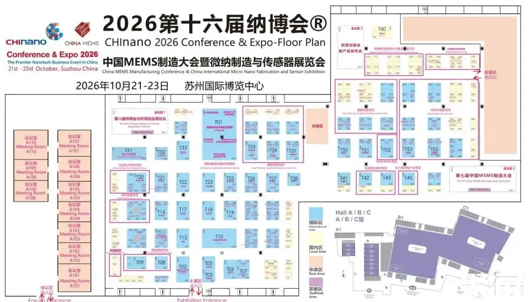
CHInano 2026 Venue Map
China (Suzhou) International Nanotechnology Industry Expo Range
- Nano-new Materials ,
- Nanoscale Microspheres ,
- Nano-coatings ,
- Nano-composite Materials ,
- Production Equipment ,
- Dispersion Technologies ,
- Analytical and Testing Instruments ,
- New Energy Technologies ,
- PM2.5 Prevention Devices ,
- Consumables
- MEMS Processing Equipment ,
- Nanoimprint Technology ,
- Microfabrication Technologies ,
- Analysis and Testing ,
- MEMS Devices ,
- MEMS Devices and Applications ,
- MEMS Fusion and Bonding Technologies ,
- Next-generation Lithography Technologies
- Gallium Nitride (GaN) and Silicon Carbide (SiC) ,
- Gallium Oxide ,
- Aluminum Nitride ,
- Diamond and Other Third-generation Semiconductor Substrates ,
- Epitaxial Materials ,
- Photoresist ,
- Photomasks ,
- CMP Polishing Materials ,
- Photoresist Materials ,
- Wet Electronic Chemicals ,
- Semiconductor Manufacturing ,
- Packaging ,
- Other Electronics-specific Equipment ,
- Compound Semiconductor RF Devices ,
- Power Devices ,
- LED Lighting and Displays ,
- Upstream and Downstream Industry Chain ,
- Innovative Applications
- Atomic Force Microscopes ,
- Backscatter Detectors ,
- Metallographic Microscopes ,
- Polarizing Microscopes ,
- Fluorescence Microscopes ,
- Electron Microscopes ,
- Mass Spectrometers ,
- Raman Microscopes ,
- Biological Microscopes ,
- Transmission Electron Microscopes ,
- Multiphoton Imaging Microscopes ,
- FEG Desktop Scanning Electron Microscopes ,
- Scanning Electrochemical Microscopes ,
- Materials Characterization ,
- Intelligent Fluorescence Microscopy Systems ,
- Electron Microscopy Inspection ,
- Blue-light 3D Scanners
- Miniature Sensors ,
- Controllers ,
- Actuators ,
- High-performance Motors ,
- Drives ,
- Communication Modules ,
- Robot Joints ,
- Power Transmission ,
- Biomimetic Skin Materials ,
- Speech Capture/Recognition ,
- Haptic Feedback ,
- Gesture Recognition ,
- LiDAR ,
- Robots for Various Application Scenarios
- Silicon, Germanium, and Other Semiconductor Materials ,
- Rare Metal Materials ,
- Compound Semiconductor Materials ,
- Dielectric Materials ,
- Piezoelectric and Ferroelectric Materials ,
- Conductive Metals and Their Alloys ,
- Magnetic Materials ,
- Optoelectronic Materials ,
- Electromagnetic Wave Shielding Materials ,
- Electronic Ceramics ,
- Polymeric Materials ,
- Insulating Dielectric Materials ,
- Piezoelectric Crystal Materials ,
- Electronic Fine Chemicals ,
- Electronic Light Construction and Textiles (Electronic Textiles) ,
- Soldering ,
- PCB Manufacturing Materials ,
- Other Electronic Materials
- Tube Furnaces ,
- Box Furnaces ,
- Vacuum Sintering Furnaces ,
- Induction Furnaces ,
- Chemical Vapor Deposition (CVD) ,
- Physical Vapor Deposition (PVD) ,
- Magnetron Sputtering ,
- Electron Beam Evaporation ,
- Ball Mills/High-energy Ball Mills ,
- Electrospinning ,
- Spray Dryers ,
- 3D Printing ,
- Metal/Ceramic/Polymer Additive Manufacturing ,
- Hot Presses ,
- Precision Molding of Polymeric Materials ,
- Vacuum Systems ,
- Centrifuges ,
- Molecular Pumps ,
- Mechanical Pumps ,
- Glove Boxes ,
- Supercritical Drying Equipment ,
- Plasma Equipment ,
- Dispersion Equipment
- Optical Communication Chips ,
- Laser Chip ,
- Detector Chip ,
- Optical Switch ,
- Infrared Sensor Chip ,
- MEMS Optical Sensor Chip ,
- Semiconductor Laser ,
- Display Optoelectronic Mini/Micro LED Chips ,
- OLED Light-emitting Devices ,
- Silicon Photonics Integration ,
- Silicon Photonics Chip ,
- Silicon Photonics Module ,
- Silicon Photonics Package ,
- Optical Sensor Applications ,
- Automotive LiDAR
- G-line, I-line, KrF, ArF (Dry/Immersion), EUV Photoresists ,
- Positive/Negative Photoresists ,
- Nanoimprint Technology ,
- Stripping ,
- Specialty Photoresists ,
- Photomasks ,
- Anti-reflective Coatings ,
- Coating/Development Supporting Materials ,
- Resins ,
- Polymers ,
- Monomers ,
- Organic Solvents ,
- High-purity Reagents ,
- Electronic Specialty Gases
Booth Sales

Ms. MaoGold-Medal PM
3 Years Booth Sales

Mr. WuGold-Medal PM
3 Years Booth Sales
2026 Suzhou New Materials Ticket Sales

Mr. HanGold-Medal PM
3 Years Booth Sales

Ms. LiuGold-Medal PM
3 Years Booth Sales
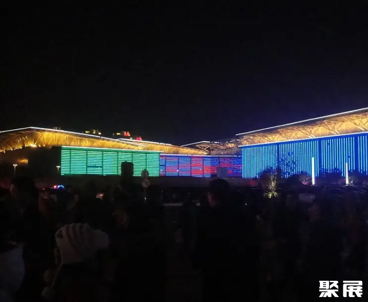
Suzhou New Materials Venue




Venue transport
- Train
From Suzhou Railway Station: Take Metro Line 4 directly from Suzhou Railway Station, ride one stop to “Leqiao Station,” then transfer to Line 1 and continue to “Cultural Expo Center Station.”
From Suzhou North Railway Station: Take Metro Line 2 to “Guangjiannan Road Station,” then transfer to Line 1 and proceed to “Cultural Expo Center Station.”
Suzhou New Materials Booth Price
Process
- 1.Submit the business license of the company
- 2.Submit product picture and name
- 3.Receive exhibition presentation documents and booth drawings
- 4.Submit booth application form/Sign booth contract
- 5.Pay the contract booth deposit
- 6.Prepare for exhibition