Bay Area Semiconductor ExpoWESEMIBAY SEMICONDUCTOR ECOSYSTEM EXPO
Bay Area Semiconductor Expo Profile
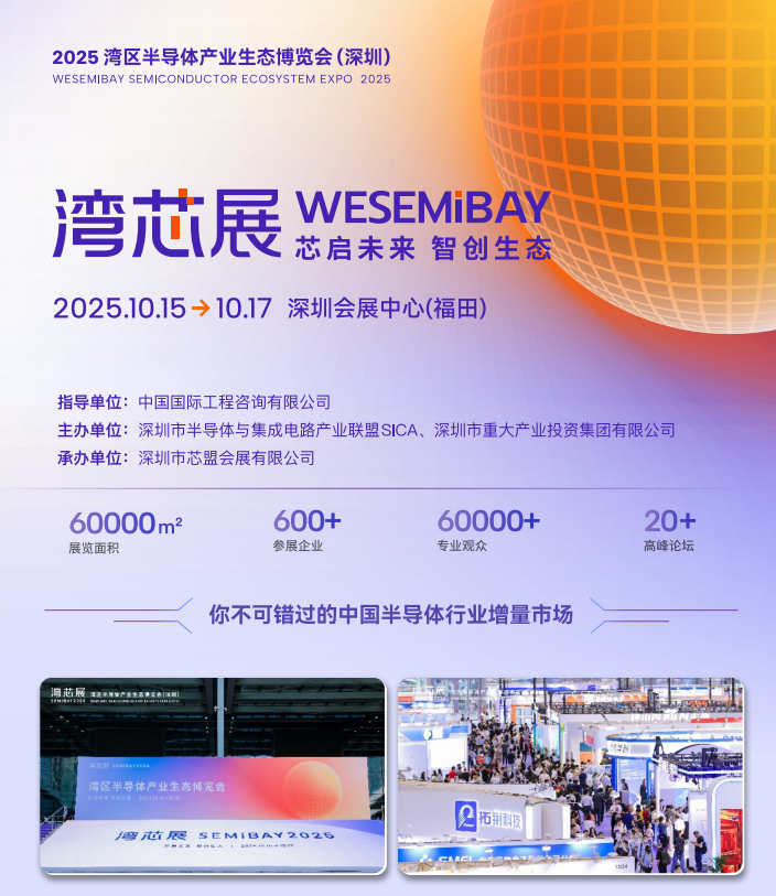
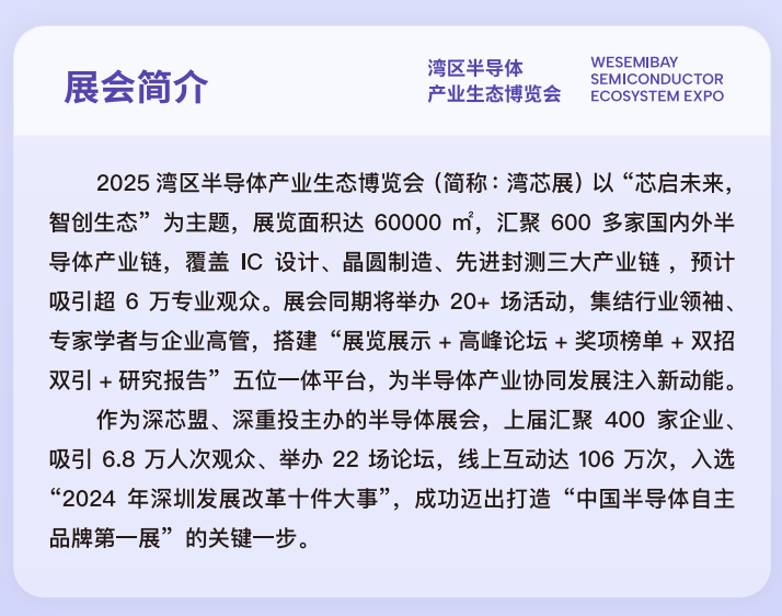
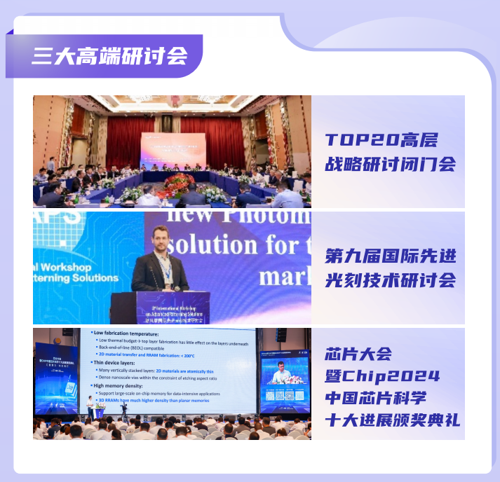
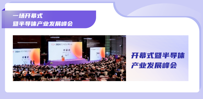
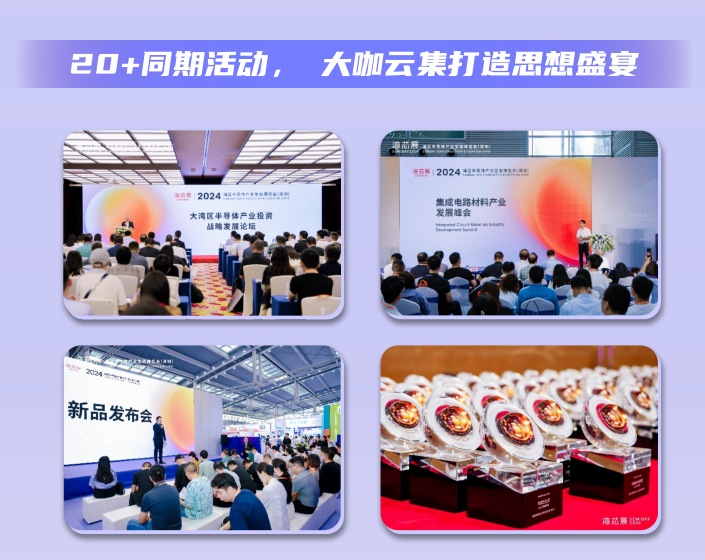
The Bay Area Semiconductor Industry Eco-Expo (abbreviated as Bay Semiconductor Expo) is themed "Chips Ignite the Future, Intelligence Creates the Ecosystem". Covering an exhibition area of 60,000㎡, it gathers over 600 leading enterprises across the domestic and international semiconductor industry chain, spanning IC design, wafer fabrication, and advanced packaging & testing. It is expected to attract over 60,000 professional visitors. Concurrently, the expo will host 20+ events, bringing together industry leaders, experts, scholars, and corporate executives to build a five-in-one platform integrating "exhibition display + high-level forums + award rankings + investment & talent attraction + research reports", injecting new momentum into the collaborative development of the semiconductor industry.
The previous edition of the Bay Semiconductor Expo received high praise from People's Daily and Xinhua News Agency for its outstanding performance, achieving a "strong start and exceeding expectations". As a top-tier domestic semiconductor exhibition organized by the Shenzhen Semiconductor Alliance, the previous edition gathered 400 enterprises, attracted 68,000 visitors, hosted 22 forums, and achieved 1.06 million online interactions. It was selected as one of the "Top 10 Major Events in Shenzhen's Development and Reform in 2024", successfully taking a crucial step toward establishing itself as "China's No. 1 Exhibition for Independent Semiconductor Brands".
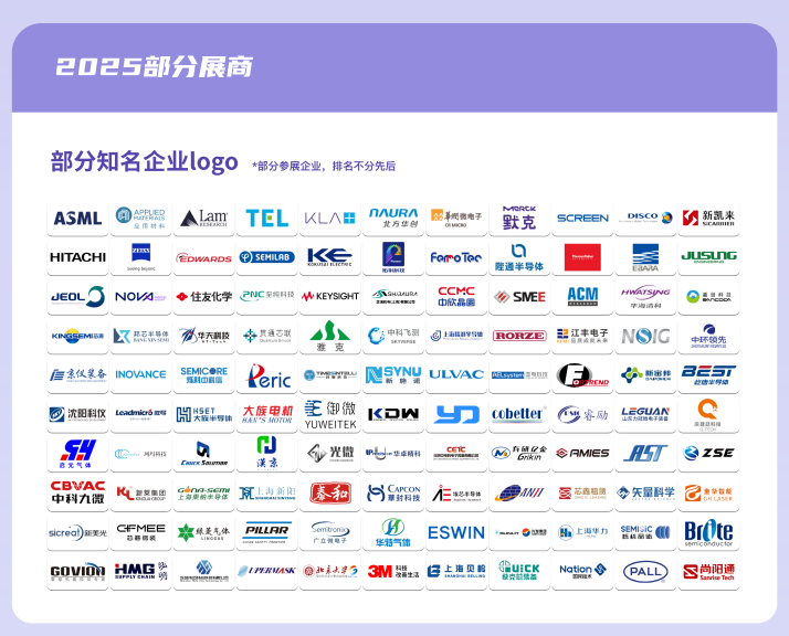
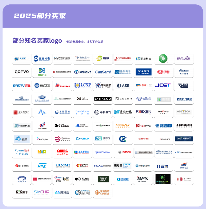
Exhibitor List
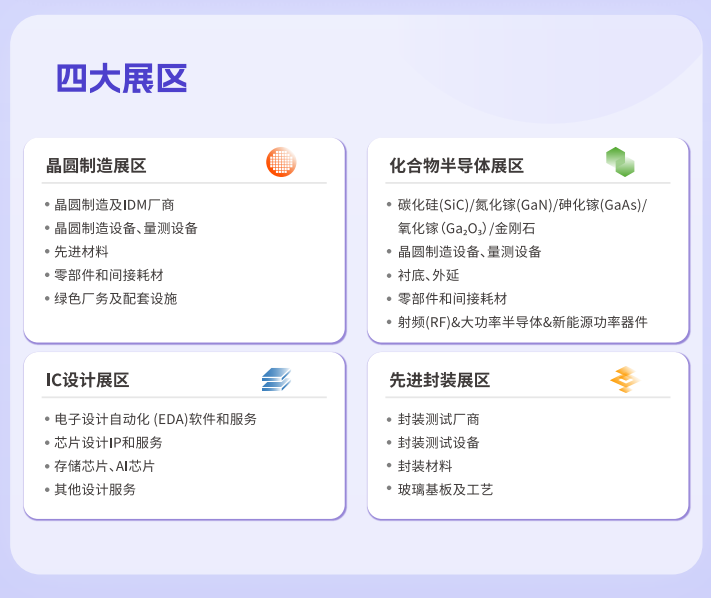
Bay Area Semiconductor Expo Product Range
Wafer Fabrication Zone: Wafer fabrication & IDM manufacturers, wafer fabrication equipment, metrology & inspection equipment, advanced materials, components & indirect consumables, green facility management & supporting infrastructure
Compound Semiconductor Zone: Silicon Carbide (SiC) / Gallium Nitride (GaN) / Gallium Arsenide (GaAs) / Gallium Oxide (Ga2O3) / Diamond, wafer fabrication equipment, metrology & inspection equipment, substrates, epitaxy, components & indirect consumables, RF & high-power semiconductors & new energy power devices
IC Design Zone: Electronic Design Automation (EDA) software & services, chip design IP & services, memory chips, AI chips, other design services
Advanced Packaging Zone: Packaging & testing manufacturers, packaging & testing equipment, packaging materials, glass substrates & processes
Bay Area Semiconductor Expo Booth Sales


Bay Area Semiconductor Expo Ticket Sales


Bay Area Semiconductor Expo Venue
Bay Area Semiconductor ExpoCommunity
Bay Area Semiconductor Expo Booth price

Standard booth Configuration
Blank booth Configuration
Bay Area Semiconductor Expo Process
1.Submit the business license of the company
2.Submit product picture and name
3.Receive exhibition presentation documents and booth drawings
4.Submit booth application form/Sign booth contract
5.Pay the contract booth deposit
6.Prepare for exhibition
Semiconductors Fair


 Online
Booth: 0571-88535771
Spectator: 0571-89099107

Online
门票咨询
Mr. Han
金牌项目经理
OnlineTel 13336023729
Mobile phone 15397162655
门票咨询
铜牌项目经理
OnlineTel 18067909721
Mobile phone 18067909721
展位咨询

Mr. Wu
金牌项目经理
OnlineTel 13867062165
Mobile phone 13867062165
Work time:Monday to Friday09:00-18:00
 My
My Ticket
- Booth apply